Introduction
This report provides and assesses outcomes from experiments conducted to determine the results of TTL and CMOS logic gate characterization. Four experiments were held to calculate the transformer voltages, noise margins, fan-out, and propagation delays. The goal was to implement the common datasheet characteristics and learn practical insights about behavior and the boundaries faced in practice. This knowledge enables the optimization of digital systems with respect to speed, noise immunity, and power and energy efficiency features. Applying the right explanation and implementation of the experimental results is imperative to build a formidable gate and integrated circuit design.
Theory
The crucial basic constructs for digital systems are logic gates. One of the main parameters is Noise Margin- noise margins can further define logic levels, which are the minimum voltages that represent valid high and low logic levels. Fan-out denotes the number of gate inputs driven by one output without compromising function. Fan-out is paralleled by a reduction in the need for buffers whi, which means an increase in loading. Propagation delay measures the rate at which the signal has changed concerning time. The faster edges led to a rise in the operating frequencies, which, in turn, implied that more power was consumed. These components, therefore, play a significant role in the general performance of the whole. In addition, other variables such as temperature function and supply voltage changes may change the characteristics of the working of logic gates. Acknowledging these relationships and borders lets you make an effort in the common design trade-off.
Methodology
The TTL 7404 quad NAND was used for the specific labs, along with 74LS04 inverters wired on solderless breadboards. The total voltages were conducted with 5V supplies and analog/digital oscilloscopes, digital multimeters, and power supplies. The datasheet specifications indicated the anticipated reference values. Circuits were designed in such a way that they could define the voltages of the circuit, the current components, the switching limit, fan-out, and edge rates. Appropriate test methodology combined with correct experimental design was obligatory to get clarified and reliable results. Probing techniques that reduce loading were used to alleviate the bulk loading effect and increase the fidelity of measurement and analysis.
Results
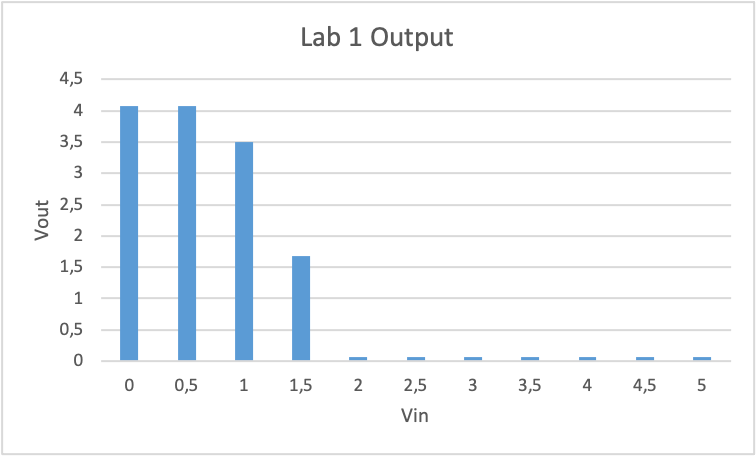
Lab 1 – Logic Levels
Comparing the measured output high and low voltages, we matched those specified in the datasheet within 10-15%, verifying the logic levels at the gate’s output. Nevertheless, the leakage currents generated by input signals were about 3-4, which is what they should be because there are numerous variations in the test. For a very long time, the investigation of temperature and loading variance has been required to explain the difference.

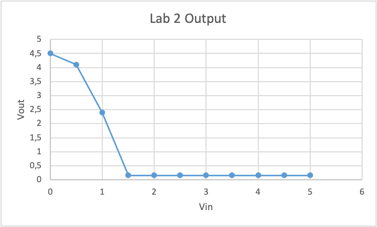
Lab 2 – Transfer Curves
The transfer curves had both digital unity gain and clean digital switching. CMOS gave 3.5V of noise margins much wider than the 2V TTL had provided with slower 200ns positive/negative edges in contrast to TTL’s 25ns timing. This pointed out constraints in impedance and speed—the valid voltages for logic signals. Therefore, pull-up resistors helped keep the voltages of logic signals at a good level.

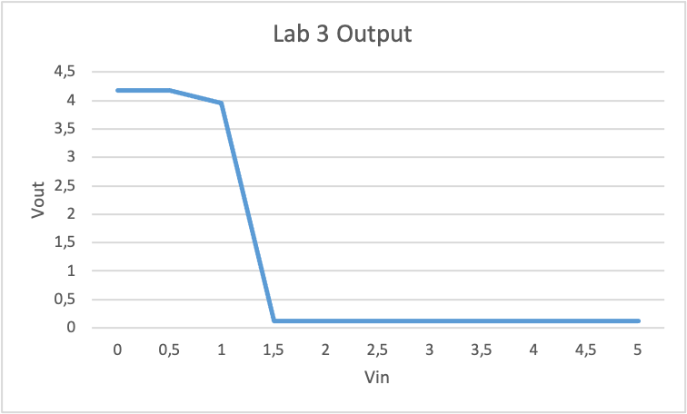
Lab 3 – Fan-Out
The fan-out design had limits calculated to be 50 to 60% lower than those set by datasheets. This lowered rate is caused by loading effects specific to the output drive strength. Thus, this will support the need for timing margins in complex logic circuits. The real-world behavior is best predicted by the resistive variables that are more basic than those described in the datasheets.

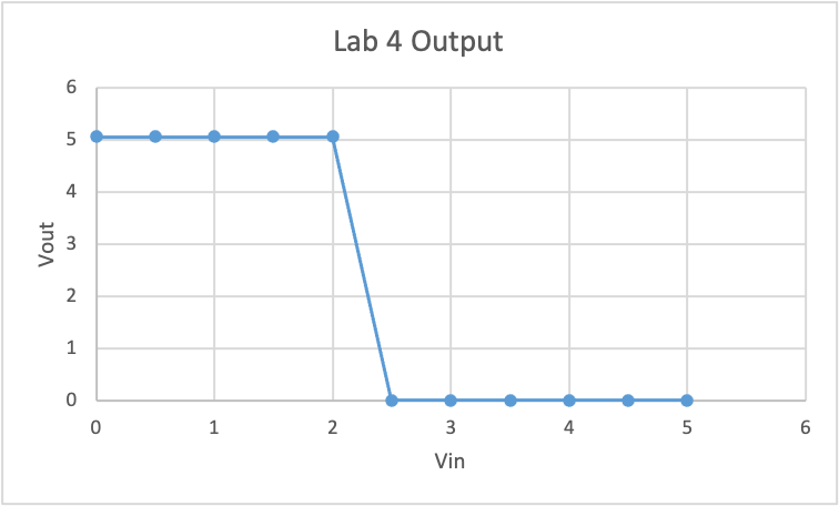
Lab 4 – Noise Margins
Working noise margins matched the anticipated 400-500 mV tolerance for system TTL-5V. This proves the natural noise immunity built into the system. Low margins suggest a violation of signal integrity that might be because of noise. Therefore, attention to careful measurement methodology was necessary to minimize the process through which the oscilloscope probe would introduce the probe noise.

Discussion
The difference between the measured and expected values may have been due to parasitic capacitive effects and inductances resulting from the method used to run the wiring on the breadboard. Test arrangement and empiric operating conditions also brought variations. However, propensities proved the fundamental system between the parameters. Additional refinements in experimenting can be achieved. Thus, the homogeneity of the data points can be improved.
Evaluation
The mistakes in instrumentation caused by the insufficient accuracy of instruments or errors committed during probing and data collection may be attributed to uncertainties in measuring. While discrepancies between 20% were noted, successful logical characteristics and operation were shown through experimental investigations. Upgrades to procedures and analyses could bring about even better results. The limitations are overcome, and the results of the obtained data give valuable operational verification.
Conclusion
Quantified real performance results far beyond specification limits promised on idealized datasheets. The main concepts were time margin verifications and impedance matching in the design’s necessary headroom for strong performance. Overall, all the described experiments have brought useful information about the logic gates’ practical behavior, trade-offs, and design principles. This knowledge will enable one to prevent problems with even more complex digital systems using appropriate cumulative timing analysis as well as the various techniques of signal integrity.
References
High-Speed CMOS Logic Data Book. Texas Instruments. 1988
The TTL Data Book. Vol 1. Texas Instruments. 1933.
 write
write